Optical Module PCB: The Ultimate Guide to Design, Fabrication, and
It will explore the complete product lifecycle, from design principles and advanced material selection to the intricacies of precision fabrication, electro-optical assembly, and quality validation.
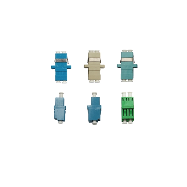
The Internal Components and Structure of The Optical Transceiver
The optical module is a very important component in an optical communication system. This article will introduce you to the internal components and structure of the optical module.
Schematic view of the main components of an optical module: (a)
The key element of many deep-sea Cherenkov detectors is the so-called "optical module", a pressure-resistant glass sphere that contains photomultipliers, which are optically coupled to the...
Optical Module PCB | APTPCB
A comprehensive guide to Optical Module PCB design and manufacturing. Learn definitions, key metrics, selection trade-offs, and validation steps for high-speed transceivers.
Optical module design resources | TI
View the TI Optical module block diagram, product recommendations, reference designs and start designing.
Considerations for PCB Layout and Impedance Matching Design
This report discusses how to use the impedance transfer circuit when we connect a mismatched trace and non-terminated TOSA, as well as what we should take into consideration when we lay out the
Printed Circuit Board Architecture for the Use of Optical
An optical printed circuit board with electrical connections in the Z axis and optical connections in the X and Y axis according to the present concept is described in greater detail below.
VarioOptics-Design2
Optical PCBs in a nutshell adding photonics functionality on the board level (optical PCBs) merging photonics (waveguides) & electronics (PCB)
Embedded Optical Interconnects in PCBs for Ultra High
Anyone that works with optical components and who is looking to
Simulation of 1.6T optical module
Today, let''s talk about why we only simulate the passive method instead of the active method to see the eye diagram. The following is a partial design circuit diagram of one of our 1.6T
Embedded Optical Interconnects in PCBs for Ultra High Speed Design
Anyone that works with optical components and who is looking to commercialize new products with optical interconnects can benefit from the full suite of PCB design tools in Altium
Telecom Racks & Cabinets
19-inch racks, wall-mount cabinets, open frames with high load capacity and seismic rating.
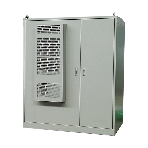
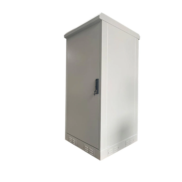
Outdoor Climate Cabinets
IP55/IP66 outdoor enclosures with integrated cooling/heating, -40°C to +55°C operation.
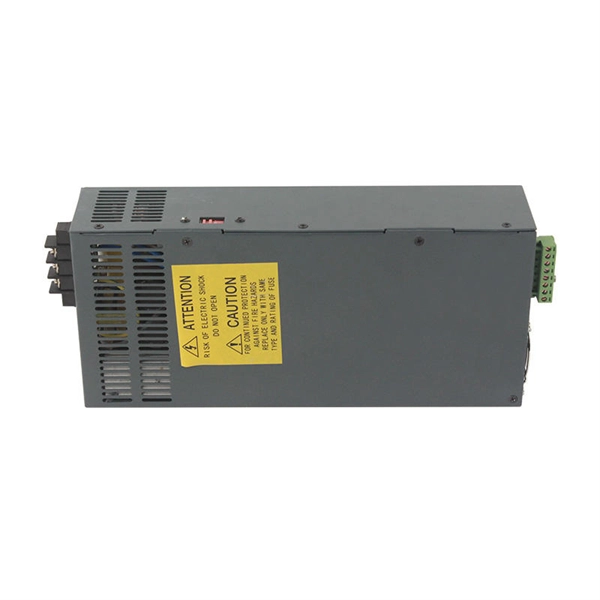
Smart PDUs & Power Distribution
Intelligent PDUs with remote monitoring, per-outlet switching, and environmental sensors.
Shelters & Network Cabinets
Prefabricated telecom shelters, emergency comms shelters, and network cabinets with cable management.